Laser shaping established as separating process for prototyping and series production
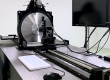
Production of optical microstructures and components at POG has become faster and more flexible. Laser-shaping now complements our traditional processing portfolio along-side wafer-dicing and mechanical edging.
Conventionally, optical microstructures and components have been cut from larger glass substrates by wafer-dicing. Parts are then centered to final diameter on CNC machines. Since both of these mechanical steps result in debris, cosmetic damage of the glass surfaces cannot be entirely avoided.
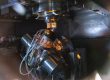
The use of laser-shaping technology enables new manufacturing opportunities. This non-ablative process is particularly suitable for products with high cleanliness requirements and for non-circular components. It is ideal for the production of coated cover glasses for the protection of sensors or for microstructures with complex outer geometries.
With our investment in laser-shaping technology, your required microstructures and plano optics can be produced even more efficiently than before – for prototyping and serial production.

Your benefits
Centering accuracy
Using the conventional centering proces-ses, it is challenging to achieve an accurate centering tolerance of the microstructure to the outer geometry, especially if there is no central structure to reference. Typical cente-ring accuracy is usually about 50μm. With laser-shaping technology, we can achieve a centering accuracy of 20μm and better (microstructured pattern to substrate profile).
diameter tolerances
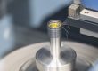
High-precision laser-shaping eliminates the need for grinding tools. Therefore, edge quality (e.g. chipping) and poor dimensional tolerances as a result of tool wear are no longer an issue. The higher shape repeatability that results from laser shaping allows tighter geometric tolerances. For substrates of 1.5mm thickness, we are able to achieve diameter tolerances of < 10μm.
Free-form 2D shaping
Laser shaping is suited for almost any two-dimensional geometry while still allowing cost-efficient separation of non-circular shaped components. For example, the production of discs with flats, components with hexagonal and octagonal shapes as well as windows with curved and free-formed edges.
Facts to know
The roughness across the traces is in the range of ≈ 1–2 μm. Separation by laser shaping is a clean and non-abrasive process which prevents edge chipping (see figures 1, 2 and 3).
It should be noted that the edges are not sharply contoured, as would be the case with a dicing or edging process. Additional costly edge bevels, e.g. to prevent injuries during handling, are unnecessary.
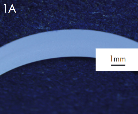
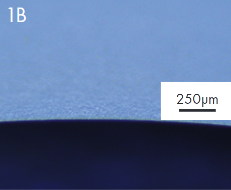
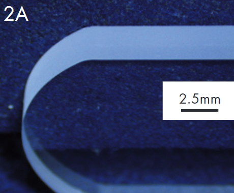
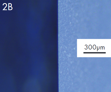
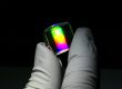
Fig. 1: Circular coverglas of B270, ø18.5 mm x 3.0 mm laser cut without macroscopic visible edge chips.
Fig. 2: Circular coverglas of B270, ø21.0 mm x 3.0 mm with 2 flats lasercut. Edge chips are not visible on a macroscopic level
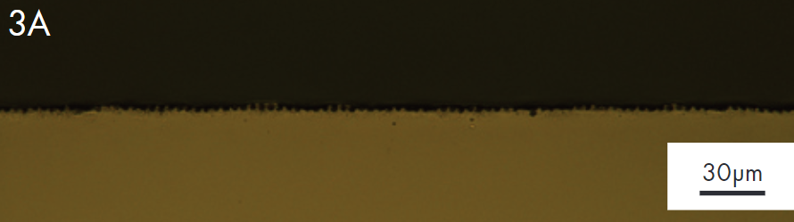
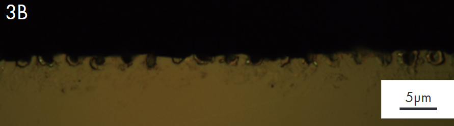
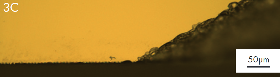
Fig. 3A and 3B: Analysis of edge quality using stereo microscopy at magnification 20x (3A) and 100x (3B). The trace of the laser can be identified, wich results in perforation-like marks of diameter < 5 μm. Edge chipping cannot be detected.
Fig. 3C: Intersection of lasercut flat with circular curvatur including protection chamfers. The laser cut flat has less chips and defects as the shape with the protection chamfers.
Conclusion
Your technological advantage
The new laser-shaping process at POG is a non-ablative process. It is a material-friendly laser technology that results in high cleanliness and improved geometric accuracies. Non-circular geometries can now also be routinely implemented for se-rial production. The manufacturing process of optical microstructures and components gains efficiency – a plus for the production of your optics.

Want to know how you can use laser shaping for your application?
Download

Please download your technology overview here for your further use.