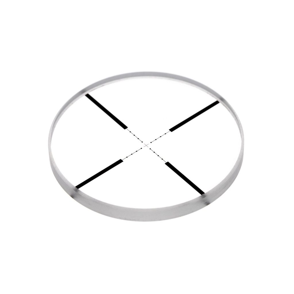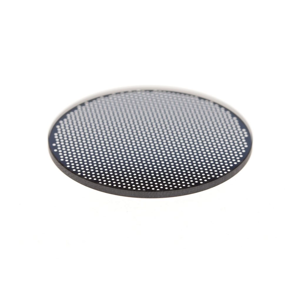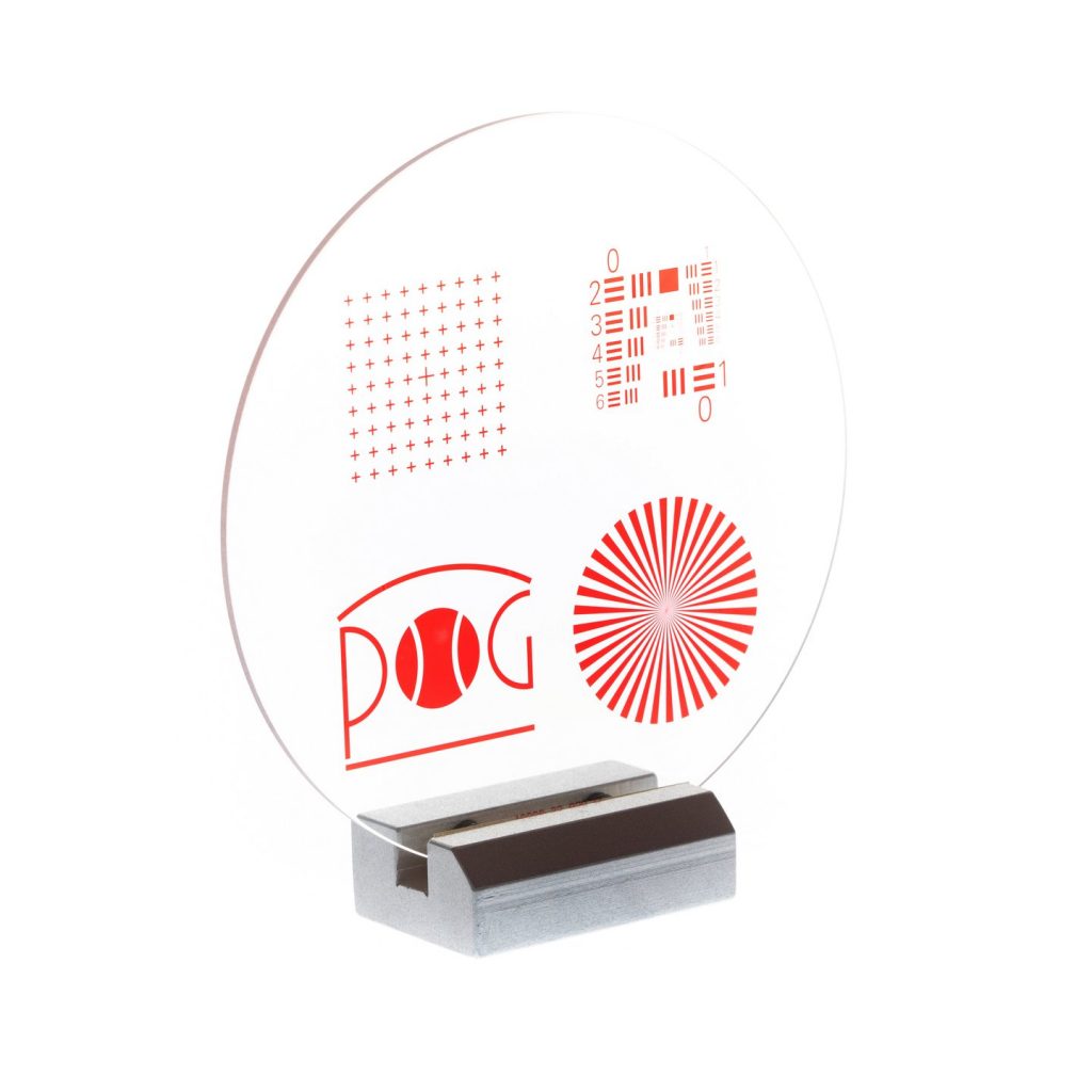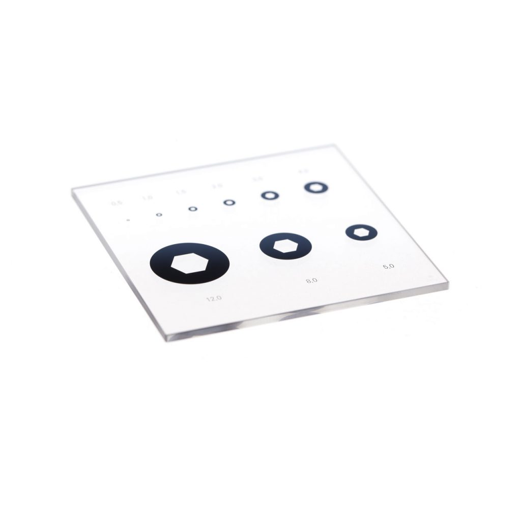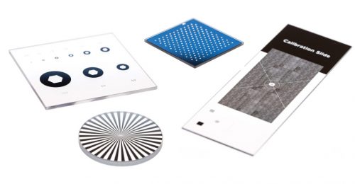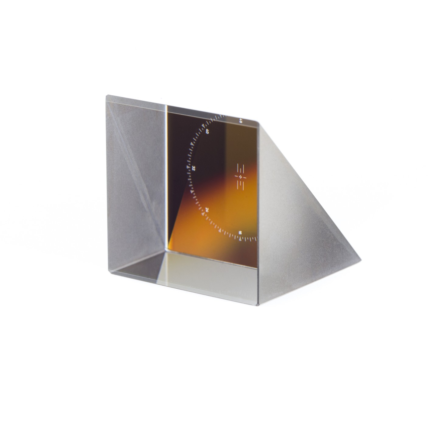
Custom solutions for custom requirements
We want to understand your specific application to be able to give you the best custom solution that fits your exact needs. Our technical sales team and process engineers help you to define the right specifications and will choose the production process that meets your needs and enables a cost efficient manufacturing for optimal quality.
Inhouse manufacturing
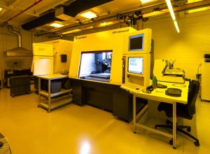
With an extensive portfolio of manufacturing technologies, we guide the production of optical microstructures entirely in-house. Our highly qualified and experienced technicians master demanding manufacturing processes from prototype to serial production quantities.
This gives us the confidence we will fulfill our promises to you – confidence on which you can rely.
Superior Product Quality
Quality is our foundation – from quotation and product design to final inspection & shipping. Documented, secure processes throughout all steps ensure the highest product quality.

Options for your custom products
You may choose from a variety of options for substrate materials, surface finishes and coatings to meet the requirements of your specific application.
We recommend below standard substrates for cost optimization.
| Substrate Material | Material Type | Substrate Thickness [mm] | Thickness Tolerances [mm] | Substrate Size [mm x mm] |
| D263 | thin glass technical float glass |
0.145 0.17 0.21; 0.3; 0.4 0.55; 0.7 |
±0.02 ±0.005 ±0.02 ±0.05 |
100×100 |
| B270 | technichal glass | 1.0; 1.5; 2.0; 3.0 | ±0.1 | 101.6 x 101.6 127 x 127 |
| SK-1300 | synthetic fused silica | 1.0; 1.5 | ±0.1 | 127 x 127 |
| Nextrema 724-8 | technical glass ceramics white opaque |
0.63; 1.0; 1.5; 2.0; 3.0 | ±0.1 | 101.6 x 101.6 127 x 127 |
Nonstandard substrate requirements can be custom prepared for our lithographic processing. Our sales team will be happy to quote your custom needs.
We offer a variety of options for metallic coatings that may be patterned to realize your product.
A major part of typical requirements may be accomplished by using one of the below standard thin film versions:
| Coating Code | Coating Material | Optical Density | Reflection | Remarks | Data Sheet |
| POG-HRC-OD3 | Chrom HRC | OD>3@550nm | R>45%@550nm | High Reflective Chrome, bright chrome, metallic gloss | POG-HRC-OD3 |
| POG-LRC-550-OD3 | Chrom LRC | OD>3@550nm | R<15%@550nm | Low Reflective Chrome, black chrome – with reflection-reducing effect in the VIS range | POG-LRC-550-OD3 |
For differing requirements reagrding optical density, reflection or spectral position further field-tested versions are available:
| Coating Code | Coating Material | Optical Density | Reflection | Remarks | Data Sheet |
| POG-HR-Al-PL | Al + SiO2 | R(abs) spec. wavelength > 90% R(avg) 400-700nm > 85% |
VIS-mirror | POG-HR-Al-PL | |
| POG-HR-Au-PL | Au + Y2O3 |
For new coatings to meet your custom requirements or in combination with special substrate materials we are glad to offer you a custom solution with an individual coating design.
We are equipped with different technologies to realize varying customer requirements. In the process of evaluating of your specific requirements we choose the optimal manufacturing process.
| Exposure Process | Image Field [mm] | Resolution Capability [µm] | Remarks |
| Mask aligner | max. 200×200 (or 8 x 8″) |
1,5 |
|
| projection copy with 1:1 projection | max. ø 80 | 5 |
|
| projection copy with 5:1 reduction | max. ø 20 | 1.0 |
|
| electron beam direct writing | max. 150×150 | 1.0 |
|
| laser exposure | ca. 150×150 | 1.0 |
|
| contact copy | approx. 200×200 | 3 to 5 |
|
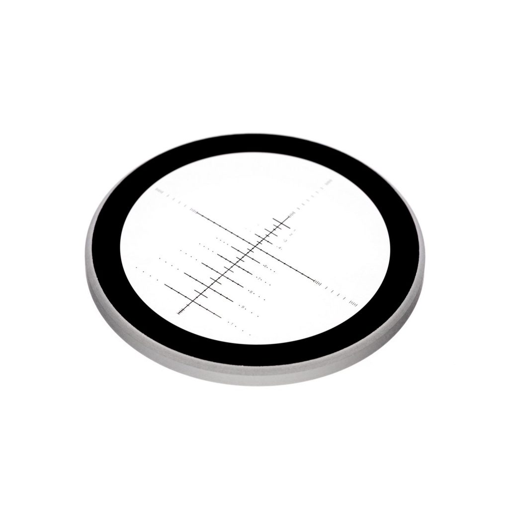
We produce pattern etched into the material by using different technologies. Main application are etch and fill illuminated reticles for rifle scopes.
| Process | Pattern Dimensions | Material | Remarks |
| HF-wet etching | > 6µm | B270 |
|
| plasma etching | > 2µm | fused silica |
|
Further details can be found here.
For most applications in the VIS area we recommend our standard broadband anti reflection coating:
| Coating Code | Reflection | AoI | Remarks | Data Sheet |
| POG-AR-420-650 | Rabs < 0.5% @ 420-650nm | 0° to 15° | POG-AR-420-650 |
For new coatings to meet your custom requirements or in combination with special substrate materials we are glad to offer you a custom solution with an individual coating design.

